270485841 © Ruslan Batiuk | Dreamstime.com


Andes/Shutterstock
66050573 © Nils Ackermann | Dreamstime.com

Recommended
Recommended
Members Only Content


SEARCH FOR DATA SHEETS, PRICE, STOCK, AND PART STATUS OF ELECTRONIC COMPONENTS
SEARCH FOR DATA SHEETS, PRICE, STOCK, AND PART STATUS OF ELECTRONIC COMPONENTS
Learning Resources
Learning Resources
Dreamstime_marcpinter_7842798


Sponsored Content
Sponsored Content
Sponsored Content
Industry Insights
Industry Insights
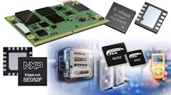
NXP Semiconductors


19425571 © Jakub Jirsak | Dreamstime.com

311250589 © Anatolii Savitskii | Dreamstime.com

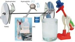
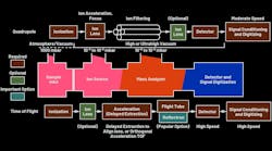
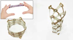
Drexel Univ/Univ of British Columbia

61664434 © Baloncici | Dreamstime.com

13484646 © Fabricio G Rauen | Dreamstime.com
Achronix and Dreamstime_funtapp_121372949

Empower Semiconductor

Dreamstime_businessrvlsoft_37267809

Educational Innovations and Science Direct


Dreamstime_biancoblue_304742382

Dreamstime_warutsintapanon_111244594


Embedded World


Vijay Deshpande
1025574 © Dana Rothstein | Dreamstime.com
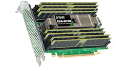
SMART Modular Technologies
Tero Vesalainen | Dreamstime.com


Dreamstime_ekkalucksangkla_1082822391


Dreamstime_pojoslaw_305383108

Dreamstime

Dreamstime_alekseigorodenkov_30

Keysight and Dreamstime_lescunliffe_23231826
Dreamstime_kiosk88generated_by_ai_11195757

Stanford University and Amazon
Cabe Atwell/Electronic Design
Muhammad Shoaib, Dreamstime
Andrei Dzemidzenka, Dreamstime

Electronic Design

Dreamstime_luchschen_26003212
Dreamstime_forfunlife_17805192